|
|
|
|
Gateway PCB
| ||
|
|
|
|
|
Gateway PCB
| ||
| Building PCB | Replacing Eth Mod Pins |
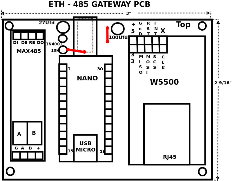
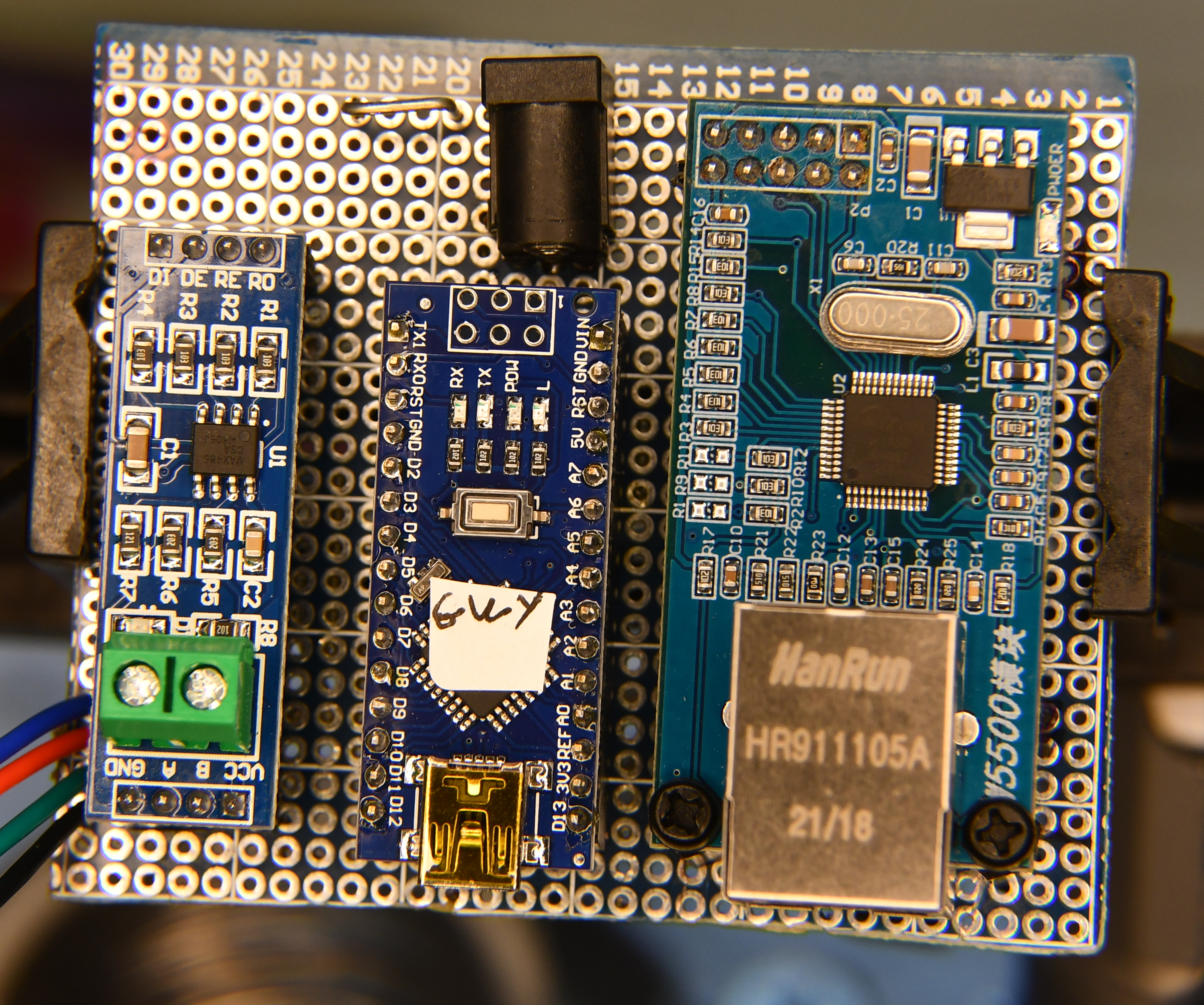
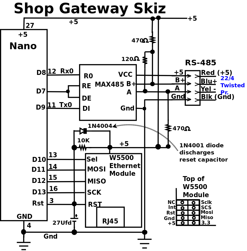
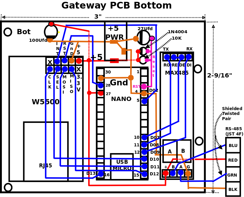
The Gateway connects our in-house network to the Shop's RS-485 network.
I did a lot of experimenting on different ethernet devices before I settled on the W5500 Module and laid out the PCB.
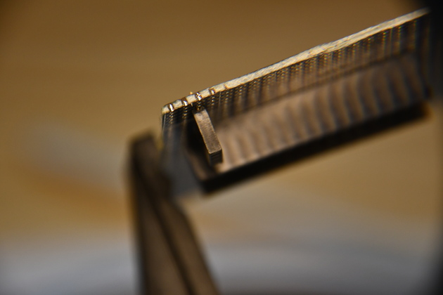
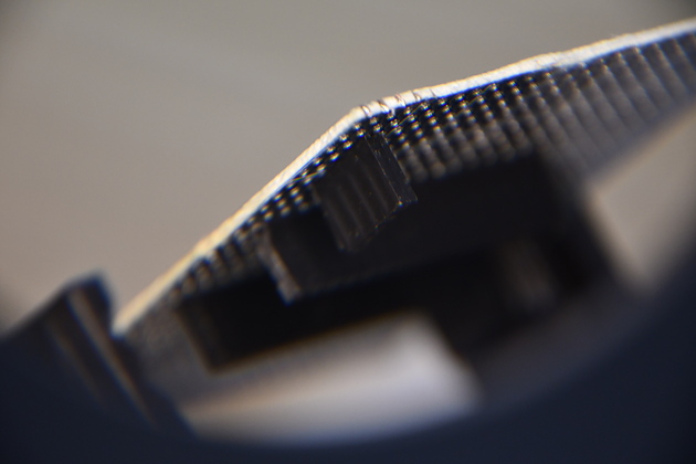
It's only problem is the pins are on the wrong side to plug it into a PCB header.
So I had to reverse them.

|

|
| ||
| Click For Larger Pic | ||||
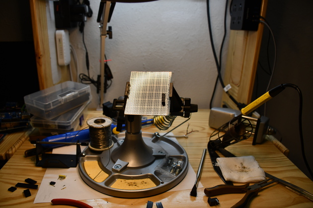
| My soldering set up on my Electronics Test Bench. You can see the PCB in the board holder with the Ethernet Module header inserted. |
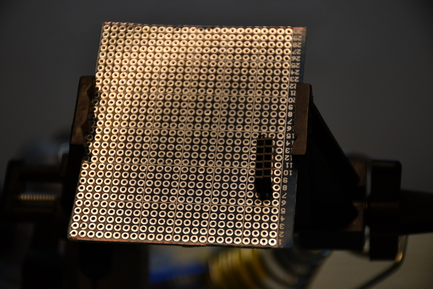
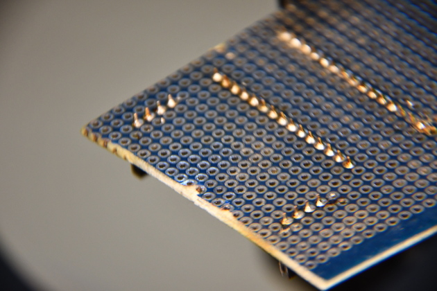
| The prototyping board, after I trimmed off the excess. Note the dual 5 pin header for the Ethernet Module, about to solder. |
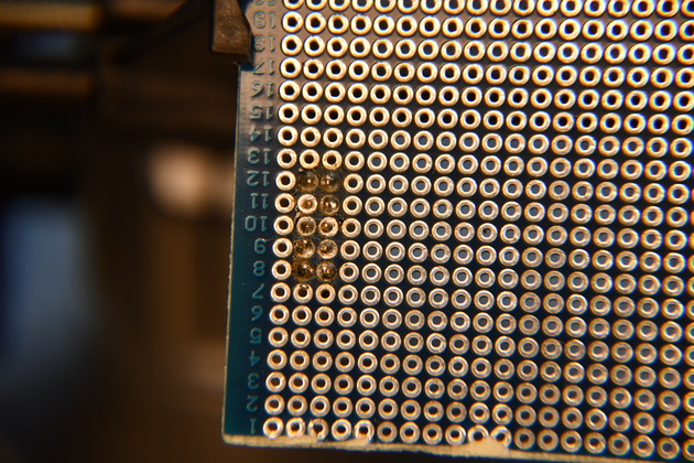
| Close look at the bottom of the prototype board, with the Ethernet Module header soldered in. |
| Now the Nano header is soldered in. Note the flux. |
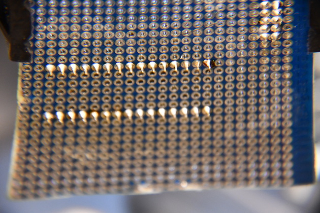
| I changed the angle so I could look for cold joints. A little Isopropyl Alcohol and an acid brush and, shazam, I can see the joints. Remember, I'm looking for cold joints and solder bridges. |
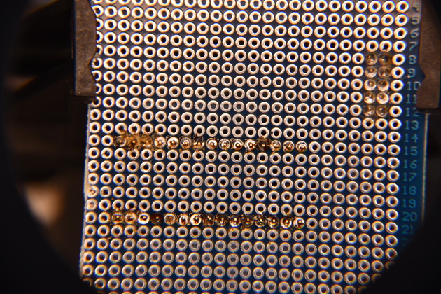
| This is how I soldered them, through my lighted magnifyer. |
| A close look at the Nano header pins. |
| Header for one end of the MAX485 board, I'm checking for vertical alignment. |
| A different angle. The in-line headers for the MAX485 and Nano. |
| Both headers for the Max485 board soldered. This is another good way to look for cold joints and solder bridges. |
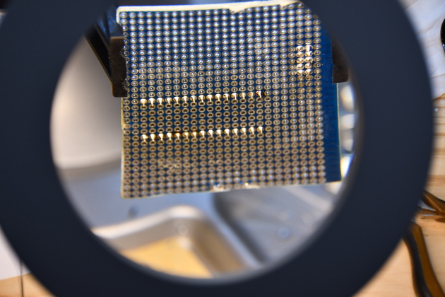
| Checking for cold joints of solder bridges. |
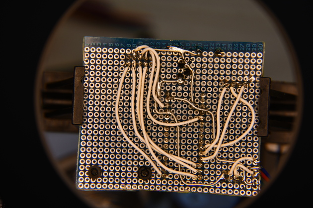
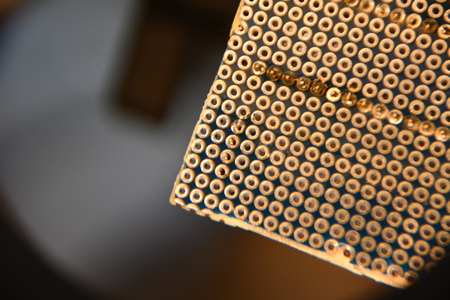
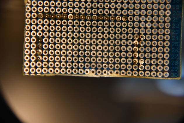
| Bottom of Gwy discrete wiring, through the magnifying glass. |
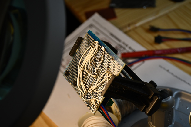
| From the side. |
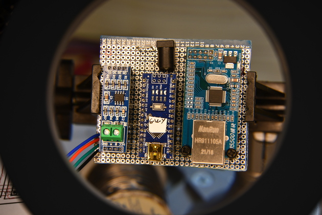
| Top of the Gwy board. |
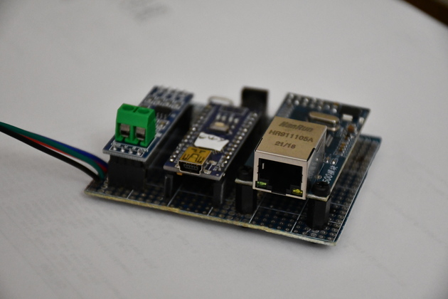
| Completed Gtw board. |

|